MODERN RADIO ENGINEERING AND TELECOMMUNICATION SYSTEMS
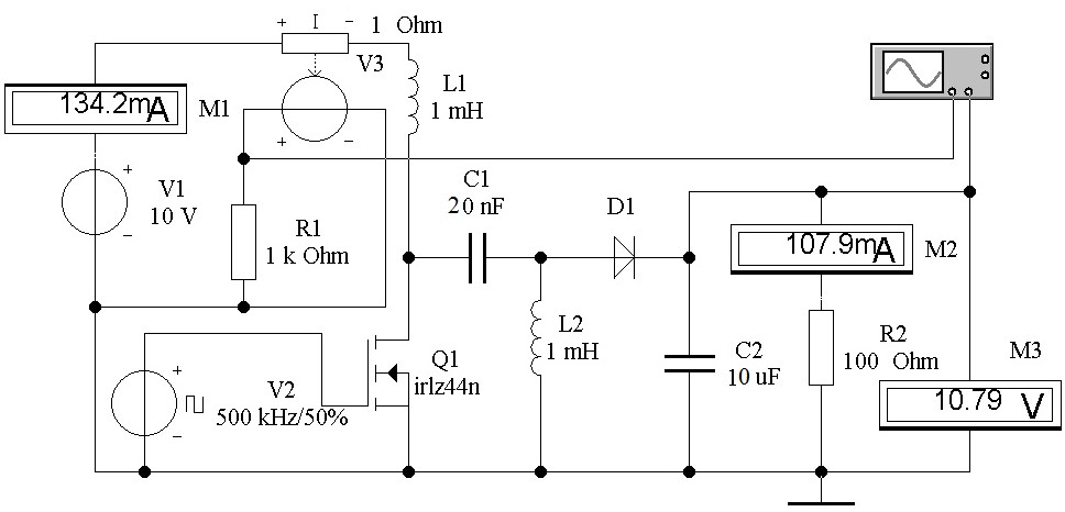
The article considers the topologies of a SEPIC buck-boost converter built according to the traditional scheme (with two inductors) and according to the scheme on magnetically coupled chokes. A circuit simulation has been done using the Electronics Workbench. The results of the investigation of a pulsed DC converter of input voltage to unipolar or bipolar output voltage using SEPIC buck-boost topology are presented. It is found that the resistance of the choke windings, which is less than 0.5 Ohm, has practically no effect on the efficiency of the converter, retaining the factor of about 0.9 in a wide range of load currents, while the main source of conversion losses is a passive diode switch. Synchronous converter circuits of a number of manufacturers are more efficient, but require more complex controllers for active switches with elements for protection against through currents.
Some advantages of the SEPIC buck-boost converter makes it stand out from other configurations. It makes possible to obtain from a unipolar input voltage both unipolar and bipolar output voltage with a good symmetry between positive and negative output voltages. It also provides efficient performance as well as circuit simplicity in unipolar and bipolar topology owing to the use of a single switch which can be operated by available integrated controllers of boost converters. The article considers the topologies of a SEPIC buck-boost converter built according to the traditional scheme (with two inductors) and according to the scheme on magnetically coupled chokes. To analyze the processes and factors affecting the converter operation efficiency, a circuit simulation has been done using the Electronics Workbench. The results of the investigation of a pulsed DC converter of input voltage to unipolar or bipolar output voltage using SEPIC buck-boost topology are presented. The circuit simulation enables to specify the switching process characteristics, to estimate the ripple level of the input current and its spectral characteristics, and to develop recommendations concerning the choice of parameters of converters elements and generation of control signals. Based on the simulation results, the load, control, and noise characteristics of the converter are obtained. The level of symmetry of positive and negative output voltage is investigated for the converter on discrete and magnetically coupled chokes. The assessment of the effect of leakage inductance on converters with magnetic coupling of inductive elements is given. Examples of practical implementation of converters built according to the SEPIC topology are shown. It is found that the resistance of the choke windings, which is less than 0.5 Ohm, has practically no effect on the efficiency of the converter, retaining the factor of about 0.9 in a wide range of load currents, while the main source of conversion losses is a passive diode switch. Synchronous converter circuits of a number of manufacturers are more efficient, but require more complex controllers for active switches with elements for protection against through currents.
For the first time, a passive method for radiosensor diagnostics of the integrity of signals from microprocessor devices was developed and presented. The method is based on the registration of the electrical component of the near field of electromagnetic radiation induced as a result of the clock formation (variability) of the impulse response of a digital circuit caused by the dynamic restructuring of the active configuration of its in-circuit and peripheral architecture. It is shown that real radiation is a superposition of fields of emitters of the active architecture of a microprocessor, each of which has its own impulse and amplitude-frequency characteristics with its own peaks and dips, resonances and excitations. It was found that the spectral-time frames of the software and hardware functioning of the digital device under study are clearly identified on the recorded radio images.
For the first time, a passive method for radiosensor diagnostics of the integrity of signals from microprocessor devices was developed and presented. The method is based on the registration of the electrical component of the near field of electromagnetic radiation induced as a result of the clock formation (variability) of the impulse response of a digital circuit caused by the dynamic restructuring of the active configuration of its in-circuit and peripheral architecture. It is shown that real radiation is a superposition of fields of emitters of the active architecture of a microprocessor, each of which has its own impulse and amplitude-frequency characteristics with its own peaks and dips, resonances and excitations. An expression of the free component is presented for the oscillatory nature of the process of energy redistribution between reactive storage devices, which depends on the capacitances of the gate dielectrics of MIS transistors, barrier and diffusion capacities of p-n junctions, inductances and ohmic resistances of circuit elements and the scheme of their architectural connection. An experiment was prepared and carried out on the method of passive radio-wave technical diagnostics of microprocessor devices on a specially developed test sample with a known command execution algorithm. The results of registration of a series of signal radio profiles when starting a sample of a digital device are presented, and a correlation assessment of the reproducibility of the experiment is carried out. It is proved that time interval transitions of free oscillations are formed on the reference signal radio profile. These transitions correspond to the microcontroller’s reference to the periphery according to the algorithm of the command functioning of the sample. The possibility of obtaining detailed information about the nature of the peripheral load and its performance by examining the corresponding sections of the reference signal radio profile is shown. It was found that the spectral-time frames of the software and hardware functioning of the digital device under study are clearly identified on the recorded radio images.
A new direction in 3D printing was investigated – prototyping of single-sided, double-sided and multilayer printed circuit boards. The first practical experience of working and printing on DragonFly LDM 2020 was presented. An additive technology for the production of multilayer printed circuit boards is considered: printing with two printheads with conductive and dielectric nano-ink with two curing systems: an infrared sintering system for conductive ink and a UV curing system for dielectric ink. The research carried out allows us to compare the technological standards of printed electronics with traditional methods of manufacturing multilayer printed circuit boards for a number of parameters.
A new direction in 3D printing was investigated – prototyping of single-sided, double-sided and multilayer printed circuit boards. The current capabilities and limitations of 3D printed circuit board printing technology were identified. A comparative analysis of the characteristics of two desktop 3D printers presented in the industry for prototyping radio electronics, as well as the first professional machine DragonFly LDM 2020, which is a mini-factory for prototyping multilayer printed circuit boards, was carried out. The first practical experience of working and printing on DragonFly LDM 2020 supplied to the megalaboratory “3D prototyping and control of multilayer printed circuit boards” of the Institute of Radio Engineering and Telecommunication Systems MIREA – Russian Technological University is presented. The first samples of electronic boards printed on a 3D printer by the method of inkjet printing were obtained. An additive technology for the production of multilayer printed circuit boards is considered: printing with two printheads with conductive and dielectric nano-ink with two curing systems: an infrared sintering system for conductive ink and a UV curing system for dielectric ink. The LDM (Dragonfly Lights-out Digital Manufacturing) production method with the necessary maintenance is presented. The method allows the system to work roundthe-clock with minimal human intervention, significantly increasing the productivity of 3D printing and expanding the possibilities of prototyping. The materials used for 3D printing of multilayer printed circuit boards and their characteristics were investigated: dielectric acrylate nano-ink (Dielectric Ink 1092 – Dielectric UV Curable Acrylates Ink), conducting ink with silver nanoparticles (AgCite™ 90072 Silver Nanoparticle Conductive Ink). The research carried out allows us to compare the technological standards of printed electronics with traditional methods of manufacturing multilayer printed circuit boards for a number of parameters.
The article discusses the possibilities of estimating the states vectors of observation objects with the non-Markovian approximation of the trajectories. In several cases the filtering errors exceed the errors of a single measurement. This leads to the conclusion that further modification of the algorithms is necessary.
The article discusses the possibilities of estimating the states vectors of observation objects with the nonMarkovian approximation of the trajectories. The introduction discusses the problem consisting in the fact that the use of the approximation of the trajectory of the observed object by Markov processes in some cases can lead to a discrepancy between theory and practice. In the first section, we simulate the trajectories of observed objects when approximated by a Markovian process and indicate the limitations of this approach. It is proposed to use a multidimensional Gaussian distribution law for generating the trajectory of the observed object. In the second section, a study of the accuracy characteristics of a single-position angular-rangefinder radar and a three-position rangefinder radar are considered. Algorithms α-β, Kalman and nonlinear estimation are used in the modeling as estimation algorithms in these systems. The parameters and characteristics of the simulation are given. In the third part, the results of modeling the process of estimating the location of objects of observation with trajectories of movement approximated by non-Markov processes are presented. Modeling confirms the possibility of using submitted algorithms to estimate the trajectory of a smallsized object of observation, a trajectory model of which uses a multidimensional normal distribution law. It is pointed out that in several cases the filtering errors exceed the errors of a single measurement. This leads to the conclusion that further modification of the algorithms is necessary. In the final part, a recommendation is given on how to further reduce the estimation errors when using Kalman algorithms and nonlinear estimation.
In this paper, we consider the possibilities of realizing fused single-mode multiplexers/demultiplexers based on combined fiber structures. The technology and equipment for the manufacture of these devices are presented. The optical characteristics of experimental samples of WDM-multiplexers are investigated. The results of testing for the effect of temperature are given.
One of the main directions in the development of optical communication systems is associated with the use of optical fiber (ОF) for data reception and transmission. Therefore, manufacturers began to pay special attention to the creation of new brands of OF, improving their optical and operational characteristics. This makes it possible to improve existing optical fiber components that use OF as an active medium. The most widely used are two-wavelength 1 × 2 WDM multiplexers/demultiplexers designed to separate and combine optical carriers with wavelengths of 1310 and 1550 nm, corresponding to the second and third transparency windows of quartz OF. It should be noted that multiplexers and demultiplexers are the same optical devices, which are spectrally selective splitters. Such devices are distinguished by a sufficiently high level of optical characteristics at a relatively low cost of products. However, an analysis of the multiplexers produced in recent years shows that the characteristics of these devices do not sufficiently correspond to the set of modern requirements imposed by most system developers, in particular on permissible values of external influencing factors, insertion loss and the value of optical isolation of channels. Therefore, the development and research of WDM multiplexers with improved optical characteristics is relevant. One of the possible ways of optimizing such devices using new types of OF with resistance to bending losses, of which WDM multiplexers could be made. In this paper, we consider the possibilities of realizing fused single-mode multiplexers/demultiplexers based on combined fiber structures. The technology and equipment for the manufacture of these devices are presented. The optical characteristics of experimental samples of WDM multiplexers are investigated. The results of testing for the effect of temperature are given.
The article is devoted to the issues of numerical calculation of the characteristics of the electromagnetic field of radiating apertures. This paper considers an approach to developing a computational model of a radiating aperture that may be used to calculate the characteristics of electromagnetic field in the intermediate and far zones. Examples of results obtained for circular and ring apertures describing the structure of their electromagnetic field are given. Examples of flight diagrams of a circular aperture are given. The effect of "searchlight" localization of the electromagnetic field in the intermediate zone of a circular emitting aperture is demonstrated. The effect of mutual compensation of neighbouring Fresnel zones using the circular emitting aperture model is demonstrated.
The article is devoted to the issues of numerical calculation of the characteristics of the electromagnetic field of radiating apertures. Тhe radiating aperture is a universal electrodynamic model used in the analysis of a special class of antennas, in particular, mirror and horn antennas, in the study of diffraction phenomena, in the planning of radio wave propagation paths, and when solving problems of wireless transmission of electric energy at a distance. The structure of the electromagnetic field of a radiating aperture in the intermediate and far zones is of the greatest interest according to the needs of practice. However, the theoretical solutions of these problems are usually difficult to obtain, except for some special cases related to the far zone. This leads to the development of appropriate computational models. This paper is aimed at generalization and systematization of experience in developing software for the simulation of electromagnetic field characteristics of radiating apertures in the intermediate and far zones. This paper considers an approach to developing a computational model of a radiating aperture that may be used to calculate the characteristics of electromagnetic field in the intermediate and far zones. Examples of results obtained for circular and ring apertures describing the structure of their electromagnetic field are given. Examples of flight diagrams of a circular aperture are given. The effect of “searchlight” localization of the electromagnetic field in the intermediate zone of a circular emitting aperture is demonstrated. The effect of mutual compensation of neighbouring Fresnel zones using the circular emitting aperture model is demonstrated. A program was developed for calculating the characteristics of the electromagnetic field of radiating holes in the intermediate and far zones. The results can also be used as illustration material for teaching the academic disciplines “Electrodynamics and radio wave propagation” and “Microwave devices and antennas”.
On the basis of an electrodynamic model of a screened microstrip line, built on the basis of the projection method using the Chebyshev basis, which explicitly takes into account the edge features of the field, a mathematical model of a microstrip line with a strip conductor was developed. These results make it possible to establish the limits of applicability of the quasi-static approximation and to determine the error in calculating the deceleration coefficient and wave resistance using the obtained analytical expressions. The error does not exceed 0.1%, if the width of the strip conductor is less than twice the thickness of the substrate in a wide range of changes in the substrate dielectric constant and frequency.
On the basis of an electrodynamic model of a screened microstrip line, built on the basis of the projection method using the Chebyshev basis, which explicitly takes into account the edge features of the field, a mathematical model of a microstrip line with a strip conductor was developed. The line width does not exceed the height of the substrate. In this case, the current density on the strip conductor is approximated by only one basis function. Analytical expressions are presented in the form of a sum of slowly and rapidly converging series to determine the main electrodynamic parameters of the line – wave resistance and deceleration coefficient. Due to logarithmic features, slowly converging series are summed up and transformed into rapidly converging power series. In addition, limit expressions in the form of improper integrals are given for the main electrodynamic parameters of an open microstrip line in the quasi-static approximation. Due to the logarithmic features, these integrals are also converted to rapidly converging power series. As a result, simple approximate formulas were obtained. They allow calculating the deceleration coefficient and wave impedance of the line with an error not exceeding 1%, when the width of the strip conductor is less than twice the thickness of the substrate. The results of calculating the electrodynamic parameters obtained on the basis of the developed mathematical model and on the basis of the projection method with an accuracy of up to 5 significant digits are presented. These results make it possible to establish the limits of applicability of the quasi-static approximation and to determine the error in calculating the deceleration coefficient and wave resistance using the obtained analytical expressions. The error does not exceed 0.1%, if the width of the strip conductor is less than twice the thickness of the substrate in a wide range of changes in the substrate dielectric constant and frequency.
Due to effective use of the frequency-energy resource of a radio line, considering the use of correction codes, a quite high noise immunity of radio communication systems under the influence of deliberate interference can be assured. The indicated dependences of the error probability on the signal-to-noise ratio confirm that the reliability of data transmission can be significantly increased by the proper combination of signal spectrum spreading, applying of correction codes, and frequency division of subsymbols followed by their weight processing.
In the context of continuous improvement of radio prospecting and active radio jamming technics along with introduction of automated active countermeasures systems (ACS), the frequency-hopping spread spectrum (FHSS) radio communication systems (RCS) are widely used in order to improve reliability and noise immunity of data transmission. The noise immunity of the RCS affected by unintentional or deliberate interference can be significantly perfected by the combined use of frequency-time division and antinoise coding. This paper explores the case when the interference created by an ACS system with a limited transmitter power covers a part of the RCS frequency range. The receiver gets input mix of the wanted signal, the receiver noise, and probably a deliberate interference also considered as a noise. The article analyzes the noise immunity of signals reception with FHSS in the low-speed radio systems with joint use of frequency-time division of information subsymbols and noise combating codes when the deliberate interference destructively impacts a part of the RCS working band. Dependence of the bit error probability on the signal-to-noise ratio is calculated for the joint use of frequency division of information subsymbols and noise combating codes. It is shown that due to effective use of the frequency-energy resource of a radio line, considering the use of correction codes, a quite high noise immunity of RCS under the influence of deliberate interference can be assured. The indicated dependences of the error probability on the signal-to-noise ratio confirm that the reliability of data transmission can be significantly increased by the proper combination of signal spectrum spreading, applying of correction codes, and frequency division of subsymbols followed by their weight processing.
The paper is devoted to the study of the mutual location between the road network (as exemplified by the public roads network) and cellular coverage of the Russian telecom operators on the territory of Russia. An overview of modern web services, Open Data and Open Source developments in transport projects is made. The practical part of the study shows the global transport accessibility raster datasets for the test region of Russia (Irkutsk Region, Siberian Federal District). An analysis of spatial relationships between roads and cellular coverages provided by VimpelCom/Beeline, Megafon and MTS is based on the Open Data in the Open Source GIS application QGIS. Coverage varies between 63% (VimpelCom for the buffer zone of 2.5 km) and 94% (Megafon for the zone of 10 km), where 100% is the total number of cells (polygons) within the network of a respective operator in the region.
Geographic information technologies and data are widely used to identify a variety of spatial relationships. The paper is devoted to the study of the mutual location between the road network (as exemplified by the public roads network) and cellular coverage of the Russian telecom operators on the territory of Russia. Transport researches are characterized with an emphasis of GIS projects. Then, an overview of modern web services, Open Data and Open Source developments in transport projects is made. The data, geodata services and web projects of cellular coverage for the territory of Russia are described by the examples of Russian-language sources. The practical part of the study shows the global transport accessibility raster datasets for the test region of Russia (Irkutsk Region, Siberian Federal District). An analysis of spatial relationships between roads and cellular coverages provided by VimpelCom/ Beeline, Megafon and MTS is based on the Open Data in the Open Source GIS application QGIS. Coverage varies between 63% (VimpelCom for the buffer zone of 2.5 km) and 94% (Megafon for the zone of 10 km), where 100% is the total number of cells (polygons) within the network of a respective operator in the region. We have noted that Open Data on the public road network and cellular communication for the territory of Russia differ by region, the studied communication datasets and data services do not contain significant attributive information, they consist of polygon geometry only. Frequency of their updates depends on the operating companies. The operators then provide the data for the publication to the Russian ministries and regional administrations.
The article presents a new method for diagnosing the technical condition of radio-electronic components, combining the methods of thermal diagnostics with the technologies of artificial neural networks. The structure of the method is shown, and the composition of the functional blocks is determined. The results of the study showed that the network automatically classifies the characteristic defects of electronic components using the algorithms embedded in it. The list of characteristic defects in the proposed diagnostic method is limited to a discrete set of the most common faults. The Kohonen network has the ability to convert large-dimensional input data into a two-dimensional array. So, the results are easy to visualize and convenient to use when generating reports and recommendations for subsequent decision-making about the possibility of using an electronic device.
The article presents a new method for diagnosing the technical condition of radio-electronic components, combining the methods of thermal diagnostics with the technologies of artificial neural networks. The structure of the method is shown, and the composition of the functional blocks is determined. The implementation of the method is a symbiosis of technologies for mathematical and simulation modeling of the technical state of a radio-electronic device with its physical tests and research of characteristics. When developing the method, specialized software tools for design and circuit design were actively used, such as Altium Designer CAD, SolidWorks, NI Multisim, the FloTHERM PCB thermal analysis module, as well as the MATLAB mathematical modeling and calculation package. With the help of these tools, a number of studies were carried out, including sets of numerical values of the power of circuit elements and temperature indicators of the printing unit, both for the correct state of the device and in states with artificially introduced defects. They, in turn, became the basis of the database of electronic node failures. To implement diagnostic procedures and identify the technical condition, an artificial neural network based on selforganizing Kohonen maps was created, its structure, parameters and algorithms of functioning were determined. The diagnostic procedure is based on the analysis of information from the fault database and its comparison with experimental data obtained as a result of a physical experiment. The results of the study showed that the network automatically classifies the characteristic defects of electronic components using the algorithms embedded in it. The list of characteristic defects in the proposed diagnostic method is limited to a discrete set of the most common faults, because, as their number increases, the use of the self-organizing Kohonen network for automatic classification becomes much more complicated and ineffective in terms of performance and reliability of identification. Among the advantages of this technology, it should be noted that the Kohonen network has the ability to convert largedimensional input data into a two-dimensional array. So, the results are easy to visualize and convenient to use when generating reports and recommendations for subsequent decision-making about the possibility of using an electronic device.

ISSN 2500-316X (Online)